Moderated newsgroup PARTS RECYCLING for somebody LOOKING OR SELLING.... > Metal Working Machine
> Drill Press
> In Area
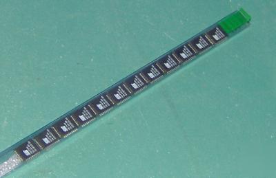
> Sst SST49LF040 flash memory devices 4 mbit lpc flash
Sst SST49LF040 flash memory devices 4 mbit lpc flash
What is for sale: Sst SST49LF040 flash memory devices 4 mbit lpc flash
– SST49LF040: 512K x8 (4 Mbit)
• Conforms to Intel LPC Interface Specification 1.0
– Uniform 64 KByte overlay blocks
– 64 KByte Top boot block protection
• Single 3.0-3.6V Read and Write Operations
– Endurance: 100,000 Cycles (typical)
– Greater than 100 years Data Retention
– Active Read Current: 6 mA (typical)
– Standby Current: 10 ?A (typical)
• Fast Sector-Erase/Byte-Program Operation
– Sector-Erase Time: 18 ms (typical)
– Block-Erase Time: 18 ms (typical)
– Chip-Erase Time: 70 ms (typical)
– Byte-Program Time: 14 ?s (typical)
– Chip Rewrite Time: 8 seconds (typical)
– Single-pulse Program or Erase
– Low Pin Count (LPC) Interface mode for
– Parallel Programming (PP) mode for fast production
– 5-signal communication interface supporting
– 33 MHz clock frequency operation
– WP# and TBL# pins provide hardware write protect
for entire chip and/or top boot block
– Data# Polling and Toggle Bit for End-of-Write
– 5 GPI pins for system design flexibility
– ID pins for multi-chip selection
– Decode both top and bottom regions of the
• Parallel Programming (PP) Mode
– 11-pin multiplexed address and 8-pin data
– Supports fast programming In-System on programmer
• CMOS and PCI I/O Compatibility
Always Read . . . THE FINE PRINT
* Returns accepted on all items unless stated, and must be arranged within stated time. Stated time starts the day you receive your item. Return for any reason if
The SST49LF040 flash memory devices are designed to
interface with the LPC bus for PC and Internet Appliance
application in compliance with Intel Low Pin Count (LPC)
Interface Specification 1.0. Two interface modes are supported
by the SST49LF040: LPC mode for In-System
operation and Parallel Programming (PP) mode to interface
The SST49LF040 flash memory devices are manufactured
with SST’s proprietary, high performance SuperFlash Technology.
The split-gate cell design and thick oxide tunneling
injector attain better reliability and manufacturability compared
with alternate approaches. The SST49LF040 device
significantly improves performance and reliability, while lowering
power consumption. The SST49LF040 device writes
(Program or Erase) with a single 3.0-3.6V power supply. It
uses less energy during Erase and Program than alternative
flash memory technologies. The total energy consumed
is a function of the applied voltage, current and time
of application. Since for any give voltage range, the Super-
Flash technology uses less current to program and has a
shorter erase time, the total energy consumed during any
Erase or Program operation is less than alternative flash
memory technologies. The SST49LF040 product provides
a maximum Byte-Program time of 20 ?sec. The entire
memory can be erased and programmed byte-by-byte typically
in 8 seconds when using status detection features
such as Toggle Bit or Data# Polling to indicate the completion
of Program operation. The SuperFlash technology provides
fixed Erase and Program time, independent of the
number of Erase/Program cycles that have performed.
Therefore the system software or hardware does not have
to be calibrated or correlated to the cumulative number of
technologies, whose Erase and Program time increase
with accumulated Erase/Program cycles.
To meet high density, surface mount requirements, the
SST49LF040 device is offered in 32-lead TSOP and 32-
lead PLCC packages. See Figures 2 and 3 for pin assignments
and Table 1 for pin descriptions.
Contact: N-graham@parts-recycling.com (Nicole Graham) (email hidden).